Yet Another FDD Swapper for Amiga
One of the most popular mods for Amiga is the addition of an FDD swapper (alternatively referred to as a boot selector). Such a device logically swaps DF0 and DF1 drives, making external drive visible as DF0, while internal drive becomes a secondary drive - DF1. This allows for loading software (which expects to be loaded from DF0) from external FDD (or, likely, Gotek interface) at boot time.
I wanted to add such a mod to my Amiga 500 (which is frequently in use these days, my kids love playing Super Frog and Lemmings), but unable to find the right mod for my Amiga 500, I designed my own using ideas from existing projects.
Swapping SEL0 and SEL1 signals
Virtually all the swappers work in the same way - by crossing ~SEL0 and ~SEL1 signals (outputs from the EVEN CIA chip), responsible for selecting a drive that we want to use at the moment (let’s call it the active drive). Typically, it’s done with a small PCB that gets plugged in between the Amiga motherboard and the EVEN CIA chip.
All the solutions available support switching between normal and swapped mode. The simplest ones directly cross ~SEL0 and ~SEL1 signals using mechanical DPDT switch. Slightly more advanced solutions
use a multiplexer chip (74HCT153, 4066 or similar) controlled with a SPST switch. I don’t like the idea of cutting any holes in the enclosure, so I skipped all the projects using mechanical switches.
Some projects use the ~RESET signal to trigger the configuration switching. This signal goes low whenever Ctrl-Amiga-Amiga key combination is pressed, it’s trivial to detect a long press and use it for switching. Also, CPU doesn’t execute any code until the keys are released, which is exactly what we want. I decided to use this exact solution, as I find it elegant and clever.
Among the projects I could find AmigaFloppySwap
is almost exactly what I want, however it uses 2 chips (ATtiny13 and 74LS153) for ~SELn swapping (and one more for internal floppy detection circuit, I’ll cover it later), I managed to roll my circuit using only a single chip - ATtiny 404 MCU. It belongs to tinyAVR 0-series of microcontrollers, equipped with Event System (EVSYS) peripheral block, which can be used to switch ~SEL0/1 signals without additional multiplexer chip. And ATtiny 404 is only 0.60 EUR, as of this writing.
Internal FDD as DF1
Swapping ~SEL0/1 signals is enough for the external FDD to work as DF0. It is not enough, however, for the internal drive to work properly as DF1. This is because Amiga software performs FDD detection using a somewhat peculiar protocol (note: no detection is done for DF0, as DF0 is always present):
- turn
MTRsignal on and off for a selected drive, to reset the ID shift register (note: Amiga generates a common~MTRXsignal to enable the FDD motors, each dive should latch this signal on the falling edge of the corresponding~SELxsignal. A flip-flop forDF0motor control is part of theGARYchip). - pull
~SELxlow, read~RDYstate, and set~SELxhigh again - repeat the above step 32 times, effectively receiving 32-bit word, MSB first.
Value of this word determines the FDD type:
0x0000 0000- no drive attached (~RDYstays high all the time)0xFFFF FFFF- standard Amiga 3.5" drive0x5555 5555- Amiga 5.25" drive
What’s important is that in practice, only the 0xFFFFFFFF drive ID is used, so it suffices to pull ~RDY line low (it’s pulled up passively) whenever ~MTR signal is high, and ~SELx signal is low. You can find more details here
. For even more curious, here’s a relevant KickStart assembler code snippet
(see code from 0xFC4906 to 0xFC495A).
So if we swap ~SEL0/1 signals, we also need to add this detection circuitry for the internal drive (which is not needed when internal drive works as DF0, as it is assumed to always be present). Fortunately, all the signals needed are present on the FDD connector, all that we need is 2 open-collector NANDs like 74LS38 (one is used to invert ~SEL signal). That’s exactly how it’s done in the AmigaFloppySwap
project mentioned before.
Interestingly, Amiga 2000 includes such a circuit for its second FDD directly on the motherboard. U108 flip-flop is used to latch the _MTR state on the falling edge of _SEL1, generating motor control signal for secondary drive, U900 inverts _SEL1 and U203 open-collector NAND gate pulls _RDY low whenever motor is off and _SEL1 goes low. The sole purpose of this circuitry is detection of the second FDD by the software.
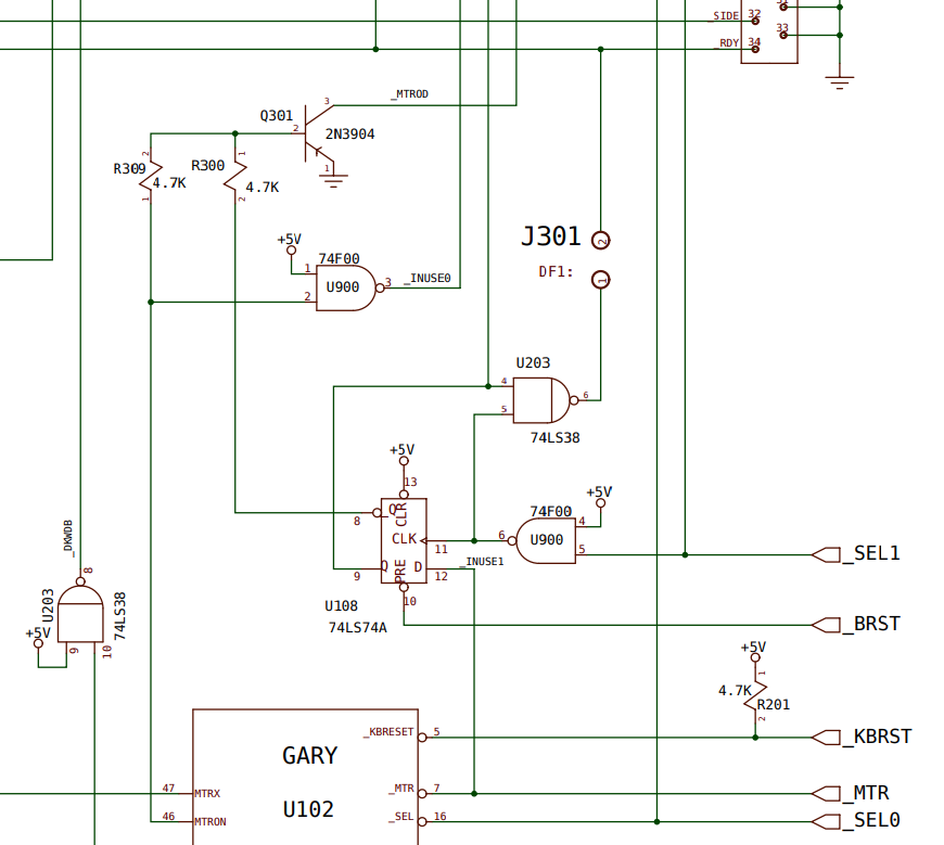
Amiga 2000 DF1 circuit.
Can we do better?
First, I don’t like how the AmigaFloppySwap
project routes MTRON and RDY between two PCBs, requiring additional wires (I guess that lack of physical space for any chip on the smaller board was the reason). We can avoid this problem entirely by moving this smaller PCB to the other end of the ribbon cable, plugging it between the motherboard and the cable. There’s plenty of space available.
Also, I’ve reached a conclusion that we can make this circuit much simpler, using just 2 MOS-FETs. Such a circuit is tiny (I’ve used transistors with SOT-23 footprints), also it doesn’t require additional power supply, which simplifies the installation - there are no extra wires to connect to the PCB at all.
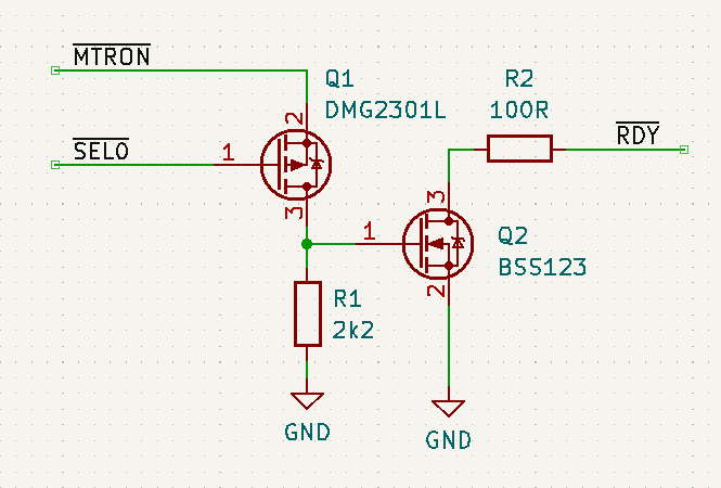
Generating RDY with MOSFETs.
Whenever ~MTRON is high and ~SEL0 is low, Q1 opens, pulling Q2’s gate high. If ~SEL0 is high, Q1 closes and R1 pulls Q2 gate down passively. It works like a charm. All the project files are available in my GitHub repo
.
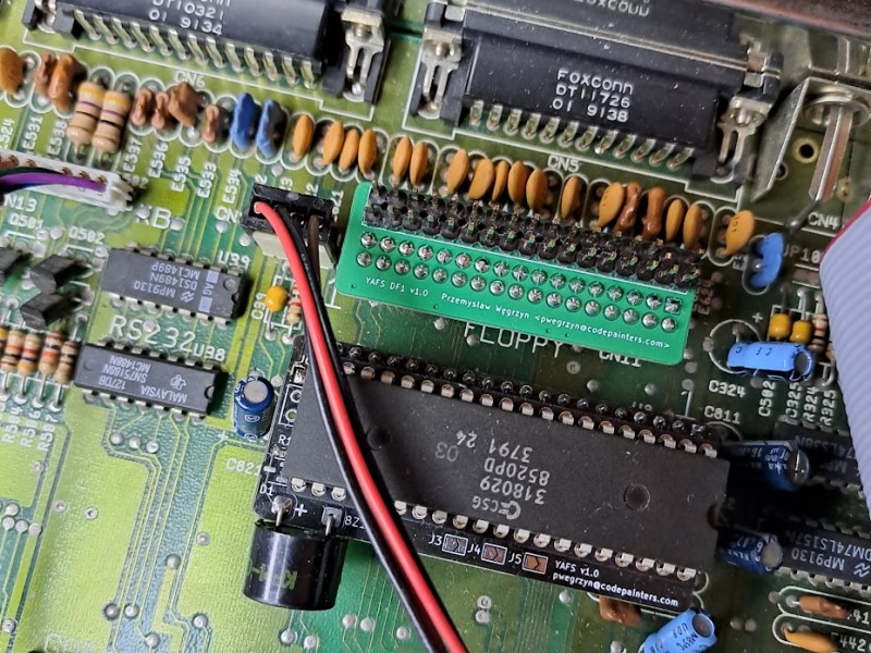
Here’s how the boards look like installed in my Amiga 500: